

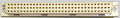
| Pin | Name |
|---|---|
| a1 | GND |
| a2 | +5V |
| a3 | +5V |
| a4 | +5V |
| a5 | /DELAY.CS |
| a6 | /VMA |
| a7 | /BG |
| a8 | /LDS |
| a9 | GND |
| a10 | A2 |
| a11 | A5 |
| a12 | A8 |
| a13 | A11 |
| a14 | A14 |
| a15 | A17 |
| a16 | reserved |
| a17 | n/c |
| a18 | reserved |
| a19 | reserved |
| a20 | D1 |
| a21 | D4 |
| a22 | D7 |
| a23 | D10 |
| a24 | D13 |
| a25 | +5/3.7V |
| a26 | A19 |
| a27 | A22 |
| a28 | FC0 |
| a29 | /IPL0 |
| a30 | /BERR |
| a31 | GND |
| a32 | GND |
| b1 | GND |
| b2 | +5V |
| b3 | +5V |
| b4 | +5V |
| b5 | /SYS.PWR |
| b6 | /BR |
| b7 | /DTACK |
| b8 | /UDS |
| b9 | +5/0V |
| b10 | A3 |
| b11 | A6 |
| b12 | A9 |
| b13 | A12 |
| b14 | A15 |
| b15 | A18 |
| b16 | reserved |
| b17 | reserved |
| b18 | reserved |
| b19 | +12V |
| b20 | D2 |
| b21 | D5 |
| b22 | D8 |
| b23 | D11 |
| b24 | D14 |
| b25 | +5V |
| b26 | A20 |
| b27 | A23 |
| b28 | FC1 |
| b29 | /IPL1 |
| b30 | /EXT.DTACK |
| b31 | 16M |
| b32 | GND |
| c1 | GND |
| c2 | +5V |
| c3 | +5V |
| c4 | +5V |
| c5 | /VPA |
| c6 | /BGACK |
| c7 | R/W |
| c8 | /AS |
| c9 | A1 |
| c10 | A4 |
| c11 | A7 |
| c12 | A10 |
| c13 | A13 |
| c14 | A16 |
| c15 | reserved |
| c16 | n/c |
| c17 | reserved |
| c18 | reserved |
| c19 | D0 |
| c20 | D3 |
| c21 | D6 |
| c22 | D9 |
| c23 | D12 |
| c24 | D15 |
| c25 | GND |
| c26 | A21 |
| c27 | E |
| c28 | FC2 |
| c29 | /IPL2 |
| c30 | /SYS.RST |
| c31 | GND |
| c32 | GND |
D0-D15
Unbuffered data bus, bits 0 through 15
A1-A23
Unbuffered address bus, bits 1 through 23
16M
16 MHz clock
/EXT.DTACK
External data transfer acknowledge. This signal is an input to the processor logic glue. Assertion delays external generation of the /DTACK signal.
E
E(enable) clock
/BERR
Bus error signal generated whenever /AS remains low for more than about 250 us.
/IPL0-/IPL2
Input priority level lines 0 through 2.
/SYS.RST
Initiates a system reset.
/SYS.PWR
A signal from the Power Manager indicated that associated circuits should tri-state their outputs and go inte idle state; /SYS.PWR is pulled high (deasserted) during sleep state.
/AS
Address strobe
/UDS
Upper data strobe
/LDS
Lower data strobe
R/W
Defines bus transfer as read or write signal
/DTACK
Data transfer acknowledge
/DELAY.CS
Indicates that a wait state is inserted into the current memory cycle and that you can delay a CS.
/BG
Bus grant
/BGACK
Bus grant acknowledge
/BR
Bus request
/VMA
Valid memory access
/VPA
Valid peripheral address
FC0-FC2
Function code lines 0 through 2
+5/0V
Provides +5V when the system is running normally and 0V when the system is in sleep mode.
+5/3.7V
Provides +5V when the system is running normally and 3.7V when the system is in sleep mode.
 correct
 incorrect