Title :
First connector:
with
x
2
3
4
5
6
7
8
9
10
11
12
13
14
15
16
17
18
19
20
21
22
23
24
25
26
28
29
30
32
34
35
36
37
38
40
42
43
44
45
46
48
50
52
54
56
58
59
60
64
68
72
74
75
80
96
98
100
116
124
132
146
152
160
164
168
172
198
240
329
pins
x pins UNKNOWN
2 pin MiniFit Jr 5557-2 female
2 pin MiniFit Jr 5566-2 male
2 pin MONO plug
2 pin motherboard fan
2 pin RCA plug
2 pin single row female
2 pin single row male
3 pin IDC male
3 pin mini-DIN female
3 pin mini-din male
3 pin motherboard fan
3 pin N3 Canon plug
3 pin RM-S1AM proprietary
3 pin single row female
3 pin single row male
3 pin stereo plug
3 pin Sub-D 3W3 female
3 pin Sub-D 3W3 male
3 pin XLR female
3 pin XLR male
4 pin 3.5mm (2.5mm) plug
4 pin Audi diagnostic
4 pin Creative SB internal
4 pin DIN 270
4 pin fan cable
4 pin Garmin proprietary
4 pin Garmin round proprietary
4 pin Head Unit LVDS shaped
4 pin HP video power
4 pin HP48 calculator proprietary
4 pin KIA HeadUnit USB
4 pin KIA LVDS display
4 pin Lowrance proprietary
4 pin Lowrance proprietary
4 pin Magellan proprietary
4 pin mini-DIN female
4 pin mini-DIN male
4 pin Mini-Molex (Berg plug)
4 pin mini-USB B
4 pin MiniFit Jr 5557-4 (molex 39-29-9042) female
4 pin MiniFit Jr 5566-4 male
4 pin Mitsubishi Head Unit USB
4 pin MOLEX 39-01-2040
4 pin MOLEX 39-29-9042
4 pin Molex power
4 pin motherboard fan
4 pin Nikon hot-shoe proprietary
4 pin Nikon MC-DC1 proprietary
4 pin Nissan Head Unit USB
4 pin Nokia external cell phone proprietary
4 pin Philips 530 cell phone proprietary
4 pin Rino proprietary
4 pin RJ11 female
4 pin RJ11 male
4 pin single row female
4 pin single row male
4 pin U-4 proprietary
4 pin uniden
4 pin USB A plug
4 pin USB A receptacle
4 pin USB B female
4 pin USB B male
4 pin XLR female
4 pin XLR male
4 pin, 6 pin or 9 pin IEEE1394 (FireWire) plug
5 pin / 4 pin mini-USB jack
5 pin / 4 pin mini-USB plug
5 pin Alcatel 311 cell phone proprietary
5 pin Alcatel BG cell phone proprietary
5 pin Apple power
5 pin DIN female
5 pin DIN male
5 pin Head Unit mini-USB
5 pin I-mobile cell phone proprietary
5 pin IDC male
5 pin Iomega proprietary
5 pin Lowrance proprietary
5 pin Micro USB A, Micro USB B plug
5 pin Micro-USB Type A, Type B receptacle
5 pin mini-din
5 pin Mini-USB type B plug
5 pin Mini-USB type B receptacle
5 pin Samsung cell phone proprietary
5 pin single row female
5 pin single row male
5 pin SQUARE female
5 pin Toyota USB plug
5 pin USB HDD case proprietary
5 pin XLR female
5 pin XLR male
6 pin 2x MOLEX 90331-0001
6 pin 4 pole 1/8 inch plug + 2 rings iPod proprietary
6 pin ATX AUX power
6 pin Can-Am Renegade diagnostic proprietary
6 pin deutsch diagnostic
6 pin DIN female
6 pin DIN male
6 pin Ford Mazda MECS diagnostic
6 pin Ford MCU/EEC diagnostic
6 pin Garmin proprietary
6 pin IDC female
6 pin IDC male
6 pin Kyocera cell phone proprietary plug
6 pin Lowrance (round) proprietary
6 pin Lowrance one-row proprietary
6 pin Lowrance round proprietary
6 pin MicroFit
6 pin mini-DIN female (PS/2 STYLE)
6 pin mini-DIN male (PS/2 STYLE)
6 pin MiniFit Jr 5557-6 (MOLEX 39-30-1060) female
6 pin MiniFit Jr 5557-6E (45559) female
6 pin MiniFit Jr 5566-6 (MOLEX 39-01-2060) male
6 pin MiniFit Jr 5566-6E (45558) male
6 pin MMJ female
6 pin MMJ male
6 pin Nissan Head Unit proprietary
6 pin RJ12 (6P6C) female
6 pin RJ12 (6P6C) male
6 pin Samsung cell phone proprietary
6 pin Simcard proprietary
6 pin single row female
6 pin single row male
6 pin Toyota 90980-10996, 90980-11728, 90980-11780, 90980-12539, 90980-12690 Radio plug
6 pin XLR female
6 pin XLR male
7 pin eSATA
7 pin female EDGE
7 pin Garmin proprietary
7 pin Lowrance proprietary
7 pin mini-DIN female
7 pin mini-DIN female (key in the center)
7 pin MM-card proprietary
7 pin NES socket proprietary
7 pin Serial ATA motherboard internal
7 pin SNES proprietary female
7 pin Toyota, Lexus 90980-12602 Radio
8 pin 4 pole plug + 4 pin iPod proprietary
8 pin Alcatel cell phone proprietary
8 pin Apple Lightning proprietary
8 pin BBK X7M proprietary
8 pin Chinese cell phone proprietary
8 pin Cowon D2
8 pin DIN female
8 pin DIN male
8 pin GM 13591516 (19353873)
8 pin GM 15357040 (12110626) square amplifier wiring harness
8 pin GM 15491286, 15134093 (13580111, 88988652) rounded amplifier wiring harness
8 pin GM 89047379 (19115652) amplifier wiring harness
8 pin Honda Head Unit Rear Camera
8 pin I-mobile cell phone proprietary
8 pin IDC female
8 pin IDC male
8 pin Mazda old Miata Head Unit
8 pin Mercedes proprietary
8 pin mini-DIN female
8 pin mini-DIN male
8 pin MiniFit Jr 5557-8 female
8 pin MiniFit Jr 5557-8E female
8 pin MiniFit Jr 5557-8E female
8 pin MiniFit Jr 5557-8SPFG (45587FG) female
8 pin MiniFit Jr 5557-8SPFG (45587SG) female
8 pin MiniFit Jr 5566-8 male
8 pin MiniFit Jr 5566-8E male
8 pin MiniFit Jr 5566-8SPFG(45586-FG) male
8 pin MiniFit Jr 5566-8SPFG(45586-SG) male
8 pin Mitsubishi Head Unit Camera
8 pin Motorola cell phone proprietary
8 pin Nikon Coolpix USB + serial plug
8 pin Nikon mini-USB proprietary
8 pin Nissan Head Unit
8 pin Powered USB
8 pin RJ45 (8P8C) female
8 pin RJ45 (8P8C) male
8 pin single row female
8 pin single row male
8 pin SMARTCARD proprietary
8 pin Sony Unilink proprietary
8 pin Toyota 90980-12221 Radio plug
8 pin Toyota Head Unit
8 pin Toyota, Lexus Radio 90980-12972
8 pin Toyota, Lexus Radio misc
8 pin TURBOVISION TV female
8 pin UC-E6 like-mini-usb proprietary
8 pin Volvo truck DLC diagnostic
5 or 3 pin Ford diagnostic
9 pin Apple mini din
9 pin D-SUB female
9 pin D-SUB male
9 pin deutsch truck diagnostic proprietary
9 pin Deutsch vehicle diagnostic proprietary receptacle
9 pin Garmin GPSMAP proprietary
9 pin J1930
9 pin Kinect proprietary cable
9 pin Kinect proprietary device
9 pin Mercedes diagnostic
9 pin mini-din female
9 pin mini-DIN female proprietary
9 pin mini-din male
9 pin mini-DIN male proprietary
9 pin Motorola cell phone proprietary
9 pin Nokia 5110 cell phone proprietary
9 pin SD-card proprietary
9 pin Sony Playstation proprietary
9 pin Subaru diagnostic
9 pin Uniden
9 pin USB 3.0 Standard-A, Standard-B Plugs and 11 pin USB 3.0 Powered-B Plug
10 pin Alcatel E801 cell phone proprietary
10 pin Audi in-dash Display
10 pin Benq cell phone proprietary
10 pin BMW moto diagnostic proprietary
10 pin CCJ DIN female
10 pin cell phone proprietary
10 pin Chinese cell phone proprietary 5x2
10 pin Creative SB 1394 proprietary
10 pin Hyundai AV
10 pin I-mobile 503 cell phone proprietary
10 pin IDC female
10 pin IDC keyed female
10 pin IDC keyed male
10 pin IDC male
10 pin Jeep Head Unit Audio
10 pin Lowrance proprietary
10 pin Mac Pro PSU C
10 pin Mac Pro PSU J1
10 pin Mac Pro PSU J2
10 pin Memory stick proprietary
10 pin micro-B USB 3.0 plug
10 pin mini-din female
10 pin mini-DIN female proprietary
10 pin MiniFit Jr 5557-10 female
10 pin MiniFit Jr 5566-10 male
10 pin Molex
10 pin Motorola 6200 cell phone proprietary
10 pin Motorola d520 cell phone proprietary
10 pin NEC N343i / Samsung D500 headset cell phone proprietary
10 pin Nikon MC-22 proprietary female
10 pin Nikon MC-22 proprietary plug
10 pin Nissan Head Unit proprietary
10 pin Nokia 7280 cell phone proprietary
10 pin Opel diagnostic
10 pin PALM proprietary
10 pin RJ50 (10P10C) male
10 pin single row female
10 pin single row male
10 pin Sony LANC proprietary
10 pin Symbol proprietary
10 pin Toyota 90980-10997, 90980-11781, 90980-11800, 90980-12540, 90980-12691 Radio plug
11 pin Enhanced Mini-USB (EMU) plug
11 pin Ericsson cell phone proprietary
11 pin HTC ExtUSB jack
11 pin Nokia 9210 cell phone proprietary
11 pin Samsung cell phone proprietary
12 pin (2 rows) Chinese cell phone proprietary
12 pin 2x MOLEX 15-48-0106
12 pin Casio EX proprietary
12 pin cell phone proprietary
12 pin Chinese cell phone proprietary
12 pin Daewoo proprietary
12 pin Ericsson cell phone proprietary
12 pin Fendt automotive diagnostic proprietary
12 pin Ford CD Changer
12 pin GM 12064799 (15305996) wiring harness
12 pin head unit proprietary
12 pin Head Unit proprietary
12 pin Honda Head Unit MIC
12 pin Hyundai car diagnostic
12 pin IDC female
12 pin IDC male
12 pin IDC male
12 pin iPAQ male proprietary
12 pin KIA amplifier
12 pin KIA Head Unit Misc
12 pin LG handsfree cell phone proprietary
12 pin Mac Pro PSU J3
12 pin MAN DLC diagnostic
12 pin Mazda old Miata Head Unit
12 pin MiniFit Jr 5557-12 female
12 pin MiniFit Jr 5566-12 male
12 pin Nissan Head Unit
12 pin Nissan NDS CD Changer
12 pin Nokia 8110 cell phone proprietary
12 pin Nokia cell phone proprietary
12 pin Olympus proprietary plug
12 pin plain cell phone proprietary
12 pin Renault car diagnostic
12 pin Siemens Lumberg cell phone proprietary
12 pin Siemens Slim Lumberg cell phone proprietary
12 pin SNES A/V female proprietary
12 pin SNES A/V male proprietary
12 pin SNES EDGE proprietary
12 pin Sony Playstation proprietary
12 pin SonyEricsson K750i cell phone proprietary
12 pin Toyota 90980-10803 plug
12 pin Toyota 90980-12183, 90980-12552 CDC plug
12 pin Toyota Head Unit CD Changer
12 pin Toyota/Lexus Head Unit proprietary
12 pin Volvo car diagnostic
12 pin XBox power supply v1.0, v1.1 proprietary
13 pin (7+6) SATA Slimline
13 pin 13W3 female
13 pin CD Changer proprietary
13 pin eSATA USB hybrid (EUHP)
13 pin Garmin proprietary
13 pin HP motherboard proprietary
13 pin Mitsubishi cell phone proprietary
13 pin Mitsubishi Cosmo cell phone proprietary
14 (2x7) pin Dodge, Chrysler, Jeep old proprietary
14 pin (2 rows) Chinese cell phone proprietary
14 pin Acura Head Unit CD Changer connector
14 pin Apple AAUI female
14 pin Apple AAUI male
14 pin Apple PowerBook video
14 pin Apple video
14 pin BOSE external Amplifier audio
14 pin Dancal cell phone proprietary
14 pin DIN male
14 pin Ericsson cell phone proprietary
14 pin GM 15488568, 7283-4490-30 (88988743)
14 pin Head Unit proprietary
14 pin Honda Head unit CN702 proprietary
14 pin HP Jornada proprietary
14 pin IDC female
14 pin IDC male
14 pin Lobster cell phone proprietary
14 pin Mercedes truck/bus diagnostic proprietary
14 pin mini-VGA
14 pin MiniFit Jr 5557-14 female
14 pin MiniFit Jr 5566-14 male
14 pin Mitsubishi Amplifier
14 pin Mitsubishi Head Unit proprietary
14 pin Molex 39-01-2140
14 pin Motorola cell phone proprietary
14 pin Nissan consult ECU diagnostic
14 pin Nokia pop-port cell phone proprietary
14 pin Panasonic cell phone proprietary
14 pin Panasonic X70 cell phone proprietary
14 pin Philips cell phone proprietary
14 pin Ricoshet SE
14 pin Siemens C30 cell phone proprietary
14 pin Siemens S40 cell phone proprietary
14 pin SONY BETAMAX female
14 pin SONY BETAMAX male
14 pin Sony CMD cell phone proprietary
15 (7+8) pin Ford old Head Unit
15 pin BMW proprietary
15 pin Cisco DB
15 pin D-SUB female
15 pin D-SUB male
15 pin Ford Car Stereo proprietary
15 pin highdensity D-SUB female
15 pin highdensity D-SUB male
15 pin Molex 67581-0000 SATA power
15 pin Molex 67582-0000 SATA plug
15 pin Motorola cell phone proprietary
15 pin Palm proprietary
16 (8+8) pin Car Stereo ISO
16 pin (10+6) Toyota Head Unit proprietary
16 pin (6+4+6) Nissan old Head Unit
16 pin (7+9) SATA micro
16 pin 2x8 unspecified proprietary
16 pin Bosch 509 cell phone proprietary
16 pin cell phone 2 rows w/antenna left proprietary
16 pin cell phone 2 rows w/antenna right proprietary
16 pin cell phone proprietary
16 pin Clarion Head Unit proprietary
16 pin Clarion proprietary
16 pin DAF diagnostic cable
16 pin DAF/Scania diagnostic receptacle
16 pin Dell dimension PSU connector
16 pin Ford 3U2Z-14S411-DPA(B) Amp
16 pin GM 13568240, 7283-9284-80 (89047196) amplifier wiring harness
16 pin GM 15394150 harness amplifier
16 pin GM 15466054, 13568239, 7283-9078-80 (15136074)
16 pin GM 15489823, 6098-4798 (15134091) rounded amplifier
16 pin GM 15491285, 7283-9076-30 (15136073) amplifier wiring harness
16 pin GM 7283-5534-60 (89047090) amplifier harness
16 pin Honda, Mitsubishi Head Unit Aux
16 pin IDC female
16 pin IDC male
16 pin J1962 OBD-2 car diagnostic
16 pin Jeep Chrysler Head Unit Amlifier Audio
16 pin KIA amplifier
16 pin KIA monitor
16 pin Kia Radio Stereo
16 pin Mazda Head Unit proprietary
16 pin Mercedes diagnostic
16 pin MiniFit Jr 5557-16 female
16 pin MiniFit Jr 5566-16 male
16 pin NEC cell phone proprietary
16 pin Nissan Head Unit Navi/Misc
16 pin Nissan Head Unit pre-amp
16 pin Nissan old Head Unit
16 pin old Ford Head Unit
16 pin PALM proprietary
16 pin PalmOne Treo 650 proprietary
16 pin Pantech proprietary
16 pin Qualcomm cell phone proprietary
16 pin Radio Head Unit proprietary
16 pin Sharp GX10 cell phone proprietary
16 pin Toyota, Lexus 90980-12553 Radio
17 pin BMW Car Stereo proprietary
17 pin CFAST
17 pin Honda Head Unit Audio
17 pin Motorola V60 cell phone proprietary
17 pin Toyota diagnostic
18 pin Audi Audio amplifier
18 pin Car Stereo proprietary
18 pin cell phone 2 rows proprietary
18 pin DMPORT receptacle ( Hirose ST60-18P(50) )
18 pin Head Unit AV Misc
18 pin Hyundai Head Unit
18 pin Kia Head Unit A
18 pin LG B1200 cell phone proprietary
18 pin LG plain cell phone proprietary
18 pin MiniFit Jr 5557-18 female
18 pin MiniFit Jr 5566-18 male
18 pin Mitsubishi Amplifier Audio
18 pin Mitsubishi Head Unit
18 pin NEC N610 cell phone proprietary
18 pin Philips 659 cell phone proprietary
18 pin Phillips cell phone proprietary
18 pin Sagem cell phone proprietary
18 pin Samsung cell phone proprietary
18 pin Samsung right-to-left numbering cell phone proprietary
18 pin Samsung SGH-600 cell phone proprietary
18 pin SATA Express motherboard
18 pin Sony cell phone proprietary
18 pin unspecified cell phone proprietary
18 pin Vitelcom cell phone proprietary
18 pin xD card proprietary
19 pin D-SUB female
19 pin D-SUB male
19 pin HDMI type A plug
19 pin HDMI type A receptacle
19 pin Micro-HDMI (type D)
19 pin mini-HDMI (type C) plug
19 pin Philips 630 cell phone proprietary
19 pin Samsung PDA proprietary
20 pin Apple HDI-20
20 pin Apple Thunderbolt
20 pin BMW OBD2 diagnostic proprietary
20 pin Bosh cell phone proprietary
20 pin DisplayPort plug
20 pin EDGE
20 pin GM 13593932, 15491304 (15126710) Head Unit misc
20 pin GM 15491305, 13593933 (15126709) Head Unit misc
20 pin GM old proprietary
20 pin Honda Head Unit Aux
20 pin Honda Head unit CN701 proprietary
20 pin Hyundai/Kia display
20 pin ICC female
20 pin ICC male
20 pin IDC female
20 pin IDC male
20 pin Kia diagnostic proprietary
20 pin MDR20 female
20 pin MiniFit Jr 5557-20 female (MOLEX 39-01-2200)
20 pin MiniFit Jr 5566-20 male (MOLEX 39-29-9202)
20 pin Mitsubishi Head Unit
20 pin Nissan Head Unit Audio main
20 pin Samsung cell phone proprietary
20 pin Samsung E910 cell phone proprietary
20 pin Samsung ST-50 proprietary
20 pin SFF-8784 edge
20 pin single row female
20 pin single row male
20 pin Toyota 90980-12460 Radio plug
20 pin Toyota Head Unit audio
20 pin Toyota/Lexus Head Unit accesory proprietary
21 pin KIA new head unit
21 pin SCART female
21 pin SCART male
22 (8+6+8) pin Ford old premium
22 pin Audiovox cell phone proprietary
22 pin Dodge, Chrysler, Jeep car stereo
22 pin Dodge, Jeep Head Units
22 pin JVC receiver QAM1436 proprietary
22 pin KIA amplifier
22 pin male Himalaya proprietary
22 pin Maxon cell phone proprietary
22 pin MiniFit Jr 5557-22 female
22 pin MiniFit Jr 5566-22 male
22 pin MOLEX 39-01-2220
22 pin MOLEX 39-29-9222
22 pin smartmedia proprietary
23 pin BOSE external Amplifier audio
23 pin D-SUB female
23 pin D-SUB male
23 pin Samsung S100 cell phone proprietary
23 pin Toyota diagnostic
24 (8+6+8+2) pin Ford Premium old Car Stereo
24 pin Amiga 3000T power
24 pin Amphenol male
24 pin cell phone unspecified proprietary
24 pin CENTRONICS female
24 pin DVI-D female
24 pin DZM 12 DREH
24 pin Ford 9U2Z-14S411-YA Radio Plug
24 pin Ford ACM Head Unit
24 pin Ford Car Stereo proprietary
24 pin GM 12110206 car stereo harness
24 pin GMC 12110244, 12110088 (15306210) Radio Harness
24 pin HeadUnit additional
24 pin Honda 2015+ Head Unit
24 pin Honda Head Unit Audio
24 pin Honda Head Unit Aux
24 pin Hyundai Head Unit
24 pin Kia Head Unit B
24 pin LG 7050 cell phone proprietary
24 pin LG 7050 cell phone proprietary right-to-left numbering
24 pin Mazda Head Unit proprietary
24 pin MiniFit Jr 5557-24 female (MOLEX 39-01-2240)
24 pin MiniFit Jr 5566-24 male (MOLEX 44206-0007)
24 pin Molex 43025-2400 Micro-Fit
24 pin Pantech cell phone proprietary
24 pin Samsung cell phone proprietary
24 pin Samsung E530 cell phone proprietary
24 pin SUN aux power
24 pin Toyota 90980-12554 Radio plug
24 pin USB-C
24 pin USB-C plug
24 pin USB-C receptacle
25 pin Cisco DB
25 pin D-SUB female
25 pin D-SUB male
26 (10+8+8) pin ISO 10487 Head Unit / Car Audio
26 pin Asus MyPal proprietary
26 pin D-SUB
26 pin Ford ACM Head Unit
26 pin hi-density D-SUB
26 pin IDC female
26 pin IDC male
26 pin KIA amplifier
26 pin LG cell phone proprietary
26 pin SFF-8088 Mini-SAS external
26 pin Sun AUI
26 pin Toshiba proprietary
26 pin Volkswagen Head Unit Video
28 pin (24+4) Lenovo Onelink
28 pin KIA amplifier A
28 pin KIA amplifier B
28 pin Nissan Head Unit Aux
28 pin Toyota 90980-12555 Radio plug
28 pin Toyota, Lexus 82824-52380 Radio
28 pin Toyota, Lexus 90980-12760 Radio
29 pin ATI proprietary
29 pin DVI female
29 pin GM 160014-0001, 13506123
29 pin GM 160014-0002, 13506123
29 pin GM 160014-0003, 13506123
29 pin GM 160014-0004, 13506123
29 pin SAS drive
29 pin SAS SFF-8482 drive cable
24+6 pins DELL PSU male (FCI PowerBlade 51721 series)
30 pin (14+16) Chevrolet Car Stereo proprietary
30 pin Apple HDI-30
30 pin Apple iPod proprietary dock
30 pin iPOD proprietary
30 pin IVECO diagnostic
30 pin MOLEX MicroCross female
30 pin MOLEX MicroCross male
30 pin PDMI male
30 pin PSA (Peugeot-Citroen) diagnostic
30 pin Samsung Galaxy Tab proprietary
30 pin SIMM
30 pin Toyota 90980-12979 Amplifier plug
30 pin Toyota, Lexus 90980-12761 Radio
32 pin Audi Amplifier
32 pin Ford new ACM Head Unit
32 pin GM 12110115
32 pin Honda Head Unit
32 pin Mini-DVI
32 pin Nissan Head Unit Additional
32 pin SAS internal SFF-8484 female
32 pin SAS internal SFF-8484 male edge
32 pin SATA Express cable (host receptacle)
34 pin IDC female
34 pin IDC male
34 pin M/34 female
34 pin M/34 male
34 pin male EDGE
34 pin SFF-8470 Infiniband CX4 female
34 pin V.35 Cisco
35 pin Apple ADC "MicroCross" female
35 pin Apple ADC "MicroCross" male
35 pin EDGE
35 pin MOLEX "MicroCross" female
35 pin MOLEX "MicroCross" male
36 (20+8+8) pin Head Unit / Car Stereo ISO
36 pin CENTRONICS female
36 pin CENTRONICS male
36 pin D-SUB? female
36 pin Dell Axim proprietary
36 pin half-pitch Centronics (HPCN36) MDR 36 male
36 pin MDR36 female
36 pin MDR36 SGI female
36 pin Mini-SAS SFF-8087 internal plug
36 pin PCI-Express x1
36 pin SFF-8643 Internal HD Mini SAS plug
36 pin SFF-8643 Mini SAS HD socket
36 pin SFF-8644 Mini SAS HD external plug
36 pin SFF-8644 Mini SAS HD external receptacle
37 pin Cisco DB
37 pin D-SUB female
37 pin D-SUB male
37 pin MAN DLC diagnostic proprietary
38 pin Audi Amplifier
38 pin Iveco proprietary diagnostic
38 pin Mercedes X11/4 diagnostic
38 pin Slim SAS SFF-8654 4i
40 (16+12+12) pin QuadLock Fakra Head Unit / Car Stereo
40 (16+12+12) pin QuadLock Fakra plug (Opel numbering)
40 pin ASUS proprietary
40 pin Dell Axim proprietary
40 pin hi-density D-SUB female
40 pin hi-density D-SUB male
40 pin IDC female
40 pin IDC male
40 pin Nissan Head Unit Video
40 pin Toshiba proprietary
42 pin (8+8+18+8) Mercedes Comand ISO / proprietary
43 pin SAS Multilink SFF-8630 drive plug
44 pin GM RADPB-44-1AK (88988902) Head Unit
44 pin IDC (2 mm pitch) female
44 pin IDC (2 mm pitch) male
45 pin Apple HDI-45
46 (8+8+10+20) pin ISO 10487 Head Unit / Car Stereo
48 pin Apple ATA
50 pin Amphenol female
50 pin Amphenol male
50 pin CompactFlash female
50 pin D-SUB female
50 pin D-SUB male
50 pin Half Pitch Centronics female
50 pin Half Pitch Centronics male
50 pin hi-density D-SUB female
50 pin hi-density D-SUB male
50 pin IDC female
50 pin IDC male
50 pin M/50 female
50 pin M/50 male
52 pin Dodge, Jeep, Chrysler Head Unit
52 pin mini-PCIE edge pcb
52 pin Volkswagen Quadlock
54 pin Ford APIM module
56 pin JAMMA proprietary
58 pin EDGE female
58 pin EDGE male
59 pin DMS-59
59 pin Toyota, Lexus 90980-12964 Mark Levinson Radio
60 pin BURNDY (C-60)
60 pin Cisco DB
60 pin CNR bus
60 pin IDC female
60 pin IDC male
60 pin LFH-60 male
60 pin Molex 70928 HD Sub-D
64 (32+32) pin Ford new ACM Head Unit
64 pin IDC female
64 pin IDC male
64 pin PCI-Express 4x
68 pin female
68 pin hi-density D-SUB female
68 pin hi-density D-SUB male
68 pin male
68 pin Slimline
68 pin Toshiba ss3380 replicator
68 pin U.2 (SFF-8639) SATA Express
72 pin 2x36 EDGE female
72 pin SIMM
74 pin (38+35) KIA Head Unit
75 pin M.2 Edge (B and M notched)
80 pin SCSI SCA-2 female
96 pin DIN 41612 (3x32) female
96 pin Euro-DIN
96 pin male or female (Fujitsu FCN 234P096-G/Y)
98 pin (62+36)ISA EDGE female
98 pin (62+36)ISA EDGE male
98 pin PCI-Express 8x
100 pin Mini-PCI Type I/II (Amp 353183-8)
116 pin MCA bus
124 pin (98+22) PCI 5 volt EDGE
124 pin Mini-PCI Type III (Amp 1318228-1)
132 pin EDGE (AGP bus)
146 pin PC/104 16 bit
152 pin Apple Powerbook PDS
160 pin DIN 41612 (5x32) female
164 pin PCI-Express 16x
168 pin DIMM
168 pin SDRAM socket
172 pin MCA bus
198 pin (62+36/62+38) EISA EDGE
240 pin DIMM DDR2
7x47 pin (IEC917 and IEC1076-4-101)
at the
Header:
VLB=VESA Local Bus. VESA=Video Electronics Standards Association.
Content:
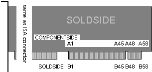
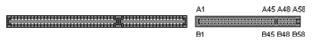
<p>The VESA Local Bus is a local bus defined by the Video Electronics Standards Association, mostly used in personal computers based on the Intel 80486 CPU. VESA Local Bus worked alongside the ISA bus; it acted as a high-speed conduit for memory-mapped I/O and DMA, while the ISA bus handled interrupts and port-mapped I/O.</p> <p>The VESA Local Bus was designed as a stop-gap solution to the problem of the ISA buss limited bandwidth. VESA had several flaws that served to limit its useful life substantially: 80486 dependence. The VESA Local Bus relied heavily on the 80486s memory bus design. When the Pentium processor started to gain mass acceptance, circa 1995, there were major differences in its bus design, and the VESA bus was not easily adaptable. This also made moving the bus to non-Intel architectures nearly impossible. Few Pentium motherboards with VESA slots were ever made. Limited number of slots available. Most PCs that used VESA Local Bus had only one or two slots available, as opposed to 5 or 6 ISA slots. This was because, as a direct branch of the 80486 memory bus, the VESA Local Bus didnt have the electrical ability to drive more than 1 or 2 (or 3 at the most) cards at a time.</p> <p>Despite these problems, the VESA Local Bus was very commonplace on 486 motherboards. Probably a majority of 486-based systems had a VESA Local Bus video card, although early 486 systems never had VESA slots, as VESA debuted years after the introduction of the 486 processor.</p> <center><img alt="" src="/images/busvlbm.gif" /></center><center> <table width="100%" cellspacing="0" cellpadding="2" border="1"> <tbody> <tr> <th>Pin</th> <th>Name</th> <th>Description</th> </tr> <tr> <td>A1</td> <td>D1</td> <td>Data 1</td> </tr> <tr> <td>A2</td> <td>D3</td> <td>Data 3</td> </tr> <tr> <td>A3</td> <td>GND</td> <td>Ground</td> </tr> <tr> <td>A4</td> <td>D5</td> <td>Data 5</td> </tr> <tr> <td>A5</td> <td>D7</td> <td>Data 7</td> </tr> <tr> <td>A6</td> <td>D9</td> <td>Data 9</td> </tr> <tr> <td>A7</td> <td>D11</td> <td>Data 11</td> </tr> <tr> <td>A8</td> <td>D13</td> <td>Data 13</td> </tr> <tr> <td>A9</td> <td>D15</td> <td>Data 15</td> </tr> <tr> <td>A10</td> <td>GND</td> <td>Ground</td> </tr> <tr> <td>A11</td> <td>D17</td> <td>Data 17</td> </tr> <tr> <td>A12</td> <td>Vcc</td> <td>+5 VDC</td> </tr> <tr> <td>A13</td> <td>D19</td> <td>Data 19</td> </tr> <tr> <td>A14</td> <td>D21</td> <td>Data 21</td> </tr> <tr> <td>A15</td> <td>D23</td> <td>Data 23</td> </tr> <tr> <td>A16</td> <td>D25</td> <td>Data 25</td> </tr> <tr> <td>A17</td> <td>GND</td> <td>Ground</td> </tr> <tr> <td>A18</td> <td>D27</td> <td>Data 27</td> </tr> <tr> <td>A19</td> <td>D29</td> <td>Data 29</td> </tr> <tr> <td>A20</td> <td>D31</td> <td>Data 31</td> </tr> <tr> <td>A21</td> <td>A30</td> <td>Address 30</td> </tr> <tr> <td>A22</td> <td>A28</td> <td>Address 28</td> </tr> <tr> <td>A23</td> <td>A26</td> <td>Address 26</td> </tr> <tr> <td>A24</td> <td>GND</td> <td>Ground</td> </tr> <tr> <td>A25</td> <td>A24</td> <td>Address 24</td> </tr> <tr> <td>A26</td> <td>A22</td> <td>Address 22</td> </tr> <tr> <td>A27</td> <td>VCC</td> <td>+5 VDC</td> </tr> <tr> <td>A28</td> <td>A20</td> <td>Address 20</td> </tr> <tr> <td>A29</td> <td>A18</td> <td>Address 18</td> </tr> <tr> <td>A30</td> <td>A16</td> <td>Address 16</td> </tr> <tr> <td>A31</td> <td>A14</td> <td>Address 14</td> </tr> <tr> <td>A32</td> <td>A12</td> <td>Address 12</td> </tr> <tr> <td>A33</td> <td>A10</td> <td>Address 10</td> </tr> <tr> <td>A34</td> <td>A8</td> <td>Address 8</td> </tr> <tr> <td>A35</td> <td>GND</td> <td>Ground</td> </tr> <tr> <td>A36</td> <td>A6</td> <td>Address 6</td> </tr> <tr> <td>A37</td> <td>A4</td> <td>Address 4</td> </tr> <tr> <td>A38</td> <td>WBACK#</td> <td>Write Back</td> </tr> <tr> <td>A39</td> <td>BE0#</td> <td>Byte Enable 0</td> </tr> <tr> <td>A40</td> <td>VCC</td> <td>+5 VDC</td> </tr> <tr> <td>A41</td> <td>BE1#</td> <td>Byte Enable 1</td> </tr> <tr> <td>A42</td> <td>BE2#</td> <td>Byte Enable 2</td> </tr> <tr> <td>A43</td> <td>GND</td> <td>Ground</td> </tr> <tr> <td>A44</td> <td>BE3#</td> <td>Byte Enable 3</td> </tr> <tr> <td>A45</td> <td>ADS#</td> <td>Address Strobe</td> </tr> <tr> <td> </td> <td> </td> <td> </td> </tr> <tr> <td>A48</td> <td>LRDY#</td> <td>Local Ready</td> </tr> <tr> <td>A49</td> <td>LDEV</td> <td>Local Device</td> </tr> <tr> <td>A50</td> <td>LREQ</td> <td>Local Request</td> </tr> <tr> <td>A51</td> <td>GND</td> <td>Ground</td> </tr> <tr> <td>A52</td> <td>LGNT</td> <td>Local Grant</td> </tr> <tr> <td>A53</td> <td>VCC</td> <td>+5 VDC</td> </tr> <tr> <td>A54</td> <td>ID2</td> <td>Identification 2</td> </tr> <tr> <td>A55</td> <td>ID3</td> <td>Identification 3</td> </tr> <tr> <td>A56</td> <td>ID4</td> <td>Identification 4</td> </tr> <tr> <td>A57</td> <td>LKEN#</td> <td> </td> </tr> <tr> <td>A58</td> <td>LEADS#</td> <td>Local Enable Address Strobe</td> </tr> <tr> <td> </td> <td> </td> <td> </td> </tr> <tr> <td>B1</td> <td>D0</td> <td>Data 0</td> </tr> <tr> <td>B2</td> <td>D2</td> <td>Data 2</td> </tr> <tr> <td>B3</td> <td>D4</td> <td>Data 4</td> </tr> <tr> <td>B4</td> <td>D6</td> <td>Data 6</td> </tr> <tr> <td>B5</td> <td>D8</td> <td>Data 8</td> </tr> <tr> <td>B6</td> <td>GND</td> <td>Ground</td> </tr> <tr> <td>B7</td> <td>D10</td> <td>Data 10</td> </tr> <tr> <td>B8</td> <td>D12</td> <td>Data 12</td> </tr> <tr> <td>B9</td> <td>VCC</td> <td>+5 VDC</td> </tr> <tr> <td>B10</td> <td>D14</td> <td>Data 14</td> </tr> <tr> <td>B11</td> <td>D16</td> <td>Data 16</td> </tr> <tr> <td>B12</td> <td>D18</td> <td>Data 18</td> </tr> <tr> <td>B13</td> <td>D20</td> <td>Data 20</td> </tr> <tr> <td>B14</td> <td>GND</td> <td>Ground</td> </tr> <tr> <td>B15</td> <td>D22</td> <td>Data 22</td> </tr> <tr> <td>B16</td> <td>D24</td> <td>Data 24</td> </tr> <tr> <td>B17</td> <td>D26</td> <td>Data 26</td> </tr> <tr> <td>B18</td> <td>D28</td> <td>Data 28</td> </tr> <tr> <td>B19</td> <td>D30</td> <td>Data 30</td> </tr> <tr> <td>B20</td> <td>VCC</td> <td>+5 VDC</td> </tr> <tr> <td>B21</td> <td>A31</td> <td>Address 31</td> </tr> <tr> <td>B22</td> <td>GND</td> <td>Ground</td> </tr> <tr> <td>B23</td> <td>A29</td> <td>Address 29</td> </tr> <tr> <td>B24</td> <td>A27</td> <td>Address 27</td> </tr> <tr> <td>B25</td> <td>A25</td> <td>Address 25</td> </tr> <tr> <td>B26</td> <td>A23</td> <td>Address 23</td> </tr> <tr> <td>B27</td> <td>A21</td> <td>Address 21</td> </tr> <tr> <td>B28</td> <td>A19</td> <td>Address 19</td> </tr> <tr> <td>B29</td> <td>GND</td> <td>Ground</td> </tr> <tr> <td>B30</td> <td>A17</td> <td>Address 17</td> </tr> <tr> <td>B31</td> <td>A15</td> <td>Address 15</td> </tr> <tr> <td>B32</td> <td>VCC</td> <td>+5 VDC</td> </tr> <tr> <td>B33</td> <td>A13</td> <td>Address 13</td> </tr> <tr> <td>B34</td> <td>A11</td> <td>Address 11</td> </tr> <tr> <td>B35</td> <td>A9</td> <td>Address 9</td> </tr> <tr> <td>B36</td> <td>A7</td> <td>Address 7</td> </tr> <tr> <td>B37</td> <td>A5</td> <td>Address 5</td> </tr> <tr> <td>B38</td> <td>GND</td> <td>Ground</td> </tr> <tr> <td>B39</td> <td>A3</td> <td>Address 3</td> </tr> <tr> <td>B40</td> <td>A2</td> <td>Address 2</td> </tr> <tr> <td>B41</td> <td>n/c</td> <td>Not connected</td> </tr> <tr> <td>B42</td> <td>RESET#</td> <td>Reset</td> </tr> <tr> <td>B43</td> <td>DC#</td> <td>Data/Command</td> </tr> <tr> <td>B44</td> <td>M/IO#</td> <td>Memory/IO</td> </tr> <tr> <td>B45</td> <td>W/R#</td> <td>Write/Read</td> </tr> <tr> <td> </td> <td> </td> <td> </td> </tr> <tr> <td>B48</td> <td>RDYRTN#</td> <td>Ready Return</td> </tr> <tr> <td>B49</td> <td>GND</td> <td>Ground</td> </tr> <tr> <td>B50</td> <td>IRQ9</td> <td>Interrupt 9</td> </tr> <tr> <td>B51</td> <td>BRDY#</td> <td>Burst Ready</td> </tr> <tr> <td>B52</td> <td>BLAST#</td> <td>Burst Last</td> </tr> <tr> <td>B53</td> <td>ID0</td> <td>Identification 0</td> </tr> <tr> <td>B54</td> <td>ID1</td> <td>Identification 1</td> </tr> <tr> <td>B55</td> <td>GND</td> <td>Ground</td> </tr> <tr> <td>B56</td> <td>LCLK</td> <td>Local Clock</td> </tr> <tr> <td>B57</td> <td>VCC</td> <td>+5 VDC</td> </tr> <tr> <td>B58</td> <td>LBS16#</td> <td>Local Bus Size 16</td> </tr> </tbody> </table> </center> <p>This section is currently based solely on the work by Mark Sokos.</p> <p>This file is intended to provide a basic functional overview of the Vesa Local Bus, so that hobbyists and amateurs can design their own VLB compatible cards.</p> <p>It is not intended to provide complete coverage of the VLB standard.</p> <p>VLB Connectors are usually inline with ISA connectors, so that adapter cards may use both. However, the VLB is separate, and does not need to connect to the ISA portion of the bus.</p> <p>The 64 bit expansion of the bus (optional) does not add additional pins or connectors. Instead, it multiplexes the existing pins. The 32 bit VLB bus does not use the 64 bit signals shown in the above pinouts.</p> <h2>Signal Descriptions</h2> <h3>A2-A31</h3> <p>Address Bus</p> <h3>ADS</h3> <p>Address Strobe</p> <h3>BE0-BE3</h3> <p>Byte Enable. Indicates that the 8 data lines corresponding to each signal will deliver valid data.</p> <h3>BLAST</h3> <p>Burst Last. Indicates a VLB Burst Cycle, which will complete with *BRDY. The VLB Burst cycle consists of an address phase followed by four data phases.</p> <h3>BRDY</h3> <p>Burst Ready. Indicates the end of the current burst transfer.</p> <h3>D0-D31</h3> <p>Data Bus. Valid bytes are indicated by *BE(x) signals.</p> <h3>D/C</h3> <p>Data/Command. Used with M/IO and W/R to indicate the type of cycle.</p> <center> <table width="100%" cellspacing="0" cellpadding="2" border="1"> <tbody> <tr> <th>M/IO</th> <th>D/C</th> <th>W/R</th> <th> </th> </tr> <tr> <td>0</td> <td>0</td> <td>0</td> <td>INTA sequence</td> </tr> <tr> <td>0</td> <td>0</td> <td>1</td> <td>Halt/Special (486)</td> </tr> <tr> <td>0</td> <td>1</td> <td>0</td> <td>I/O Read</td> </tr> <tr> <td>0</td> <td>1</td> <td>1</td> <td>I/O Write</td> </tr> <tr> <td>1</td> <td>0</td> <td>0</td> <td>Instruction Fetch</td> </tr> <tr> <td>1</td> <td>0</td> <td>1</td> <td>Halt/Shutdown (386)</td> </tr> <tr> <td>1</td> <td>1</td> <td>0</td> <td>Memory Read</td> </tr> <tr> <td>1</td> <td>1</td> <td>1</td> <td>Memory Write</td> </tr> </tbody> </table> </center> <h3>ID0-ID4</h3> <p>Identification Signals.</p> <center> <table width="100%" cellspacing="0" cellpadding="2" border="1"> <tbody> <tr> <th>ID0</th> <th>ID1</th> <th>ID4</th> <th>CPU</th> <th>Bus Width</th> <th>Burst</th> </tr> <tr> <td>0</td> <td>0</td> <td>0</td> <td>(res)</td> <td> </td> <td> </td> </tr> <tr> <td>0</td> <td>0</td> <td>1</td> <td>(res)</td> <td> </td> <td> </td> </tr> <tr> <td>0</td> <td>1</td> <td>0</td> <td>486</td> <td>16/32</td> <td>Burst Possible</td> </tr> <tr> <td>0</td> <td>1</td> <td>1</td> <td>486</td> <td>16/32</td> <td>Read Burst</td> </tr> <tr> <td>1</td> <td>0</td> <td>0</td> <td>386</td> <td>16/32</td> <td>None</td> </tr> <tr> <td>1</td> <td>0</td> <td>1</td> <td>386</td> <td>16/32</td> <td>None</td> </tr> <tr> <td>1</td> <td>1</td> <td>0</td> <td>(res)</td> <td> </td> <td> </td> </tr> <tr> <td>1</td> <td>1</td> <td>1</td> <td>486</td> <td>16/32/64</td> <td>Read/Write Burst</td> </tr> </tbody> </table> </center> <p> </p> <center> <table width="100%" cellspacing="0" cellpadding="2" border="1"> <tbody> <tr> <td>ID2 Indicates wait:</td> <td>0 = 1 wait cycle (min)</td> </tr> <tr> <td> </td> <td>1 = no wait</td> </tr> <tr> <td>ID3 Indicates bus speed:</td> <td>0 = greater than 33.3 MHz</td> </tr> <tr> <td> </td> <td>1 = less than 33.3 MHz</td> </tr> </tbody> </table> </center> <h3>IRQ9</h3> <p>Interrupt Request. Connected to IRQ9 on ISA bus. This allows standalone VLB adapters (not connected to ISA portion of the bus) to have one IRQ.</p> <h3>LEADS</h3> <p>Local Enable Address Strobe. Set low by VLB master (not CPU). Also used for cache invalidation signal.</p> <h3>LBS16</h3> <p>Local Bus Size 16. Used by slave device to indicate that it has a transfer width of only 16 bits.</p> <h3>LCLK</h3> <p>Local Clock. Runs at the same frequency as the cpu, up to 50 MHz. 66 MHz is allowed for on-board devices.</p> <h3>LDEV</h3> <p>Local Device: When appropriate address and M/IO signals are present on the bus, the VLB device must pull this line low to indicate that it is a VLB device. The VLB controller will then use the VLB bus for the transfer.</p> <h3>LRDY</h3> <p>Local Ready. Indicates that the VLB device has completed the cycle. This signal is only used for single cycle transfers. *BRDY is used for burst transfers.</p> <h3>LGNT</h3> <p>Local Grant. Indicates that an *LREQ signal has been granted, and control is being transferred to the new VLB master.</p> <h3>LREQ</h3> <p>Local Request. Used by VLB Master to gain control of the bus.</p> <h3>M/IO</h3> <p>Memory/IO. See D/C for signal description.</p> <h3>RDYRTN</h3> <p>Ready Return. Indicates VLB cycle has been completed. May precede LRDY by one cycle.</p> <h3>RESET</h3> <p>Reset. Resets all VLB devices.</p> <h3>WBACK</h3> <p>Write Back.</p> <h2>64-bit Expansion Signals</h2> <h3>ACK64</h3> <p>Acknowledge 64 bit transfer. Indicates that the device can perform the requested 64 bit transfer cycle.</p> <h3>BE4-BE7</h3> <p>Byte Enable. Indicates which bytes are valid (similar to BE0-BE3).</p> <h3>D32-D63</h3> <p>Upper 32 bits of data bus. Multiplexed with address bus.</p> <h3>LBS64</h3> <p>Local Bus Size 64 bits. Used by VLB Master to indicate that it desires a 64 bit transfer.</p> <h3>W/R</h3> <p>Write/Read. See D/C for signal description.</p> <h2>64 Bit Data Transfer Timing Diagram:</h2> <pre> Address Data Phase Phase _______ _______ _______ LCLK ___| |_______| |_______| |_______ ____ ______________________________________ *ADS |_______| _______________ _______________ A2-A31 ----<_______________><_______________>------------- D34-D63 Address Data D34-D63 _______________ _______________ D/C ----<_______________><_______________>------------- M/IO, W/R M/IO, W/R Data D32-33 _____ _____________________________ *LDEV |_______________| _____ _____________________________ *LBS64 |_______________| ______ _____________________________ *ACK64 |______________| _______________ D0-D31 --------------------<_______________>------------- _____________________ _____________ LRDY |______________|</pre> <div class="footer"> </div>
Second connector:
with
x
2
3
4
5
6
7
8
9
10
11
12
13
14
15
16
17
18
19
20
21
22
23
24
25
26
28
29
30
32
34
35
36
37
38
40
42
43
44
45
46
48
50
52
54
56
58
59
60
64
68
72
74
75
80
96
98
100
116
124
132
146
152
160
164
168
172
198
240
329
pins
x pins UNKNOWN
2 pin MiniFit Jr 5557-2 female
2 pin MiniFit Jr 5566-2 male
2 pin MONO plug
2 pin motherboard fan
2 pin RCA plug
2 pin single row female
2 pin single row male
3 pin IDC male
3 pin mini-DIN female
3 pin mini-din male
3 pin motherboard fan
3 pin N3 Canon plug
3 pin RM-S1AM proprietary
3 pin single row female
3 pin single row male
3 pin stereo plug
3 pin Sub-D 3W3 female
3 pin Sub-D 3W3 male
3 pin XLR female
3 pin XLR male
4 pin 3.5mm (2.5mm) plug
4 pin Audi diagnostic
4 pin Creative SB internal
4 pin DIN 270
4 pin fan cable
4 pin Garmin proprietary
4 pin Garmin round proprietary
4 pin Head Unit LVDS shaped
4 pin HP video power
4 pin HP48 calculator proprietary
4 pin KIA HeadUnit USB
4 pin KIA LVDS display
4 pin Lowrance proprietary
4 pin Lowrance proprietary
4 pin Magellan proprietary
4 pin mini-DIN female
4 pin mini-DIN male
4 pin Mini-Molex (Berg plug)
4 pin mini-USB B
4 pin MiniFit Jr 5557-4 (molex 39-29-9042) female
4 pin MiniFit Jr 5566-4 male
4 pin Mitsubishi Head Unit USB
4 pin MOLEX 39-01-2040
4 pin MOLEX 39-29-9042
4 pin Molex power
4 pin motherboard fan
4 pin Nikon hot-shoe proprietary
4 pin Nikon MC-DC1 proprietary
4 pin Nissan Head Unit USB
4 pin Nokia external cell phone proprietary
4 pin Philips 530 cell phone proprietary
4 pin Rino proprietary
4 pin RJ11 female
4 pin RJ11 male
4 pin single row female
4 pin single row male
4 pin U-4 proprietary
4 pin uniden
4 pin USB A plug
4 pin USB A receptacle
4 pin USB B female
4 pin USB B male
4 pin XLR female
4 pin XLR male
4 pin, 6 pin or 9 pin IEEE1394 (FireWire) plug
5 pin / 4 pin mini-USB jack
5 pin / 4 pin mini-USB plug
5 pin Alcatel 311 cell phone proprietary
5 pin Alcatel BG cell phone proprietary
5 pin Apple power
5 pin DIN female
5 pin DIN male
5 pin Head Unit mini-USB
5 pin I-mobile cell phone proprietary
5 pin IDC male
5 pin Iomega proprietary
5 pin Lowrance proprietary
5 pin Micro USB A, Micro USB B plug
5 pin Micro-USB Type A, Type B receptacle
5 pin mini-din
5 pin Mini-USB type B plug
5 pin Mini-USB type B receptacle
5 pin Samsung cell phone proprietary
5 pin single row female
5 pin single row male
5 pin SQUARE female
5 pin Toyota USB plug
5 pin USB HDD case proprietary
5 pin XLR female
5 pin XLR male
6 pin 2x MOLEX 90331-0001
6 pin 4 pole 1/8 inch plug + 2 rings iPod proprietary
6 pin ATX AUX power
6 pin Can-Am Renegade diagnostic proprietary
6 pin deutsch diagnostic
6 pin DIN female
6 pin DIN male
6 pin Ford Mazda MECS diagnostic
6 pin Ford MCU/EEC diagnostic
6 pin Garmin proprietary
6 pin IDC female
6 pin IDC male
6 pin Kyocera cell phone proprietary plug
6 pin Lowrance (round) proprietary
6 pin Lowrance one-row proprietary
6 pin Lowrance round proprietary
6 pin MicroFit
6 pin mini-DIN female (PS/2 STYLE)
6 pin mini-DIN male (PS/2 STYLE)
6 pin MiniFit Jr 5557-6 (MOLEX 39-30-1060) female
6 pin MiniFit Jr 5557-6E (45559) female
6 pin MiniFit Jr 5566-6 (MOLEX 39-01-2060) male
6 pin MiniFit Jr 5566-6E (45558) male
6 pin MMJ female
6 pin MMJ male
6 pin Nissan Head Unit proprietary
6 pin RJ12 (6P6C) female
6 pin RJ12 (6P6C) male
6 pin Samsung cell phone proprietary
6 pin Simcard proprietary
6 pin single row female
6 pin single row male
6 pin Toyota 90980-10996, 90980-11728, 90980-11780, 90980-12539, 90980-12690 Radio plug
6 pin XLR female
6 pin XLR male
7 pin eSATA
7 pin female EDGE
7 pin Garmin proprietary
7 pin Lowrance proprietary
7 pin mini-DIN female
7 pin mini-DIN female (key in the center)
7 pin MM-card proprietary
7 pin NES socket proprietary
7 pin Serial ATA motherboard internal
7 pin SNES proprietary female
7 pin Toyota, Lexus 90980-12602 Radio
8 pin 4 pole plug + 4 pin iPod proprietary
8 pin Alcatel cell phone proprietary
8 pin Apple Lightning proprietary
8 pin BBK X7M proprietary
8 pin Chinese cell phone proprietary
8 pin Cowon D2
8 pin DIN female
8 pin DIN male
8 pin GM 13591516 (19353873)
8 pin GM 15357040 (12110626) square amplifier wiring harness
8 pin GM 15491286, 15134093 (13580111, 88988652) rounded amplifier wiring harness
8 pin GM 89047379 (19115652) amplifier wiring harness
8 pin Honda Head Unit Rear Camera
8 pin I-mobile cell phone proprietary
8 pin IDC female
8 pin IDC male
8 pin Mazda old Miata Head Unit
8 pin Mercedes proprietary
8 pin mini-DIN female
8 pin mini-DIN male
8 pin MiniFit Jr 5557-8 female
8 pin MiniFit Jr 5557-8E female
8 pin MiniFit Jr 5557-8E female
8 pin MiniFit Jr 5557-8SPFG (45587FG) female
8 pin MiniFit Jr 5557-8SPFG (45587SG) female
8 pin MiniFit Jr 5566-8 male
8 pin MiniFit Jr 5566-8E male
8 pin MiniFit Jr 5566-8SPFG(45586-FG) male
8 pin MiniFit Jr 5566-8SPFG(45586-SG) male
8 pin Mitsubishi Head Unit Camera
8 pin Motorola cell phone proprietary
8 pin Nikon Coolpix USB + serial plug
8 pin Nikon mini-USB proprietary
8 pin Nissan Head Unit
8 pin Powered USB
8 pin RJ45 (8P8C) female
8 pin RJ45 (8P8C) male
8 pin single row female
8 pin single row male
8 pin SMARTCARD proprietary
8 pin Sony Unilink proprietary
8 pin Toyota 90980-12221 Radio plug
8 pin Toyota Head Unit
8 pin Toyota, Lexus Radio 90980-12972
8 pin Toyota, Lexus Radio misc
8 pin TURBOVISION TV female
8 pin UC-E6 like-mini-usb proprietary
8 pin Volvo truck DLC diagnostic
5 or 3 pin Ford diagnostic
9 pin Apple mini din
9 pin D-SUB female
9 pin D-SUB male
9 pin deutsch truck diagnostic proprietary
9 pin Deutsch vehicle diagnostic proprietary receptacle
9 pin Garmin GPSMAP proprietary
9 pin J1930
9 pin Kinect proprietary cable
9 pin Kinect proprietary device
9 pin Mercedes diagnostic
9 pin mini-din female
9 pin mini-DIN female proprietary
9 pin mini-din male
9 pin mini-DIN male proprietary
9 pin Motorola cell phone proprietary
9 pin Nokia 5110 cell phone proprietary
9 pin SD-card proprietary
9 pin Sony Playstation proprietary
9 pin Subaru diagnostic
9 pin Uniden
9 pin USB 3.0 Standard-A, Standard-B Plugs and 11 pin USB 3.0 Powered-B Plug
10 pin Alcatel E801 cell phone proprietary
10 pin Audi in-dash Display
10 pin Benq cell phone proprietary
10 pin BMW moto diagnostic proprietary
10 pin CCJ DIN female
10 pin cell phone proprietary
10 pin Chinese cell phone proprietary 5x2
10 pin Creative SB 1394 proprietary
10 pin Hyundai AV
10 pin I-mobile 503 cell phone proprietary
10 pin IDC female
10 pin IDC keyed female
10 pin IDC keyed male
10 pin IDC male
10 pin Jeep Head Unit Audio
10 pin Lowrance proprietary
10 pin Mac Pro PSU C
10 pin Mac Pro PSU J1
10 pin Mac Pro PSU J2
10 pin Memory stick proprietary
10 pin micro-B USB 3.0 plug
10 pin mini-din female
10 pin mini-DIN female proprietary
10 pin MiniFit Jr 5557-10 female
10 pin MiniFit Jr 5566-10 male
10 pin Molex
10 pin Motorola 6200 cell phone proprietary
10 pin Motorola d520 cell phone proprietary
10 pin NEC N343i / Samsung D500 headset cell phone proprietary
10 pin Nikon MC-22 proprietary female
10 pin Nikon MC-22 proprietary plug
10 pin Nissan Head Unit proprietary
10 pin Nokia 7280 cell phone proprietary
10 pin Opel diagnostic
10 pin PALM proprietary
10 pin RJ50 (10P10C) male
10 pin single row female
10 pin single row male
10 pin Sony LANC proprietary
10 pin Symbol proprietary
10 pin Toyota 90980-10997, 90980-11781, 90980-11800, 90980-12540, 90980-12691 Radio plug
11 pin Enhanced Mini-USB (EMU) plug
11 pin Ericsson cell phone proprietary
11 pin HTC ExtUSB jack
11 pin Nokia 9210 cell phone proprietary
11 pin Samsung cell phone proprietary
12 pin (2 rows) Chinese cell phone proprietary
12 pin 2x MOLEX 15-48-0106
12 pin Casio EX proprietary
12 pin cell phone proprietary
12 pin Chinese cell phone proprietary
12 pin Daewoo proprietary
12 pin Ericsson cell phone proprietary
12 pin Fendt automotive diagnostic proprietary
12 pin Ford CD Changer
12 pin GM 12064799 (15305996) wiring harness
12 pin head unit proprietary
12 pin Head Unit proprietary
12 pin Honda Head Unit MIC
12 pin Hyundai car diagnostic
12 pin IDC female
12 pin IDC male
12 pin IDC male
12 pin iPAQ male proprietary
12 pin KIA amplifier
12 pin KIA Head Unit Misc
12 pin LG handsfree cell phone proprietary
12 pin Mac Pro PSU J3
12 pin MAN DLC diagnostic
12 pin Mazda old Miata Head Unit
12 pin MiniFit Jr 5557-12 female
12 pin MiniFit Jr 5566-12 male
12 pin Nissan Head Unit
12 pin Nissan NDS CD Changer
12 pin Nokia 8110 cell phone proprietary
12 pin Nokia cell phone proprietary
12 pin Olympus proprietary plug
12 pin plain cell phone proprietary
12 pin Renault car diagnostic
12 pin Siemens Lumberg cell phone proprietary
12 pin Siemens Slim Lumberg cell phone proprietary
12 pin SNES A/V female proprietary
12 pin SNES A/V male proprietary
12 pin SNES EDGE proprietary
12 pin Sony Playstation proprietary
12 pin SonyEricsson K750i cell phone proprietary
12 pin Toyota 90980-10803 plug
12 pin Toyota 90980-12183, 90980-12552 CDC plug
12 pin Toyota Head Unit CD Changer
12 pin Toyota/Lexus Head Unit proprietary
12 pin Volvo car diagnostic
12 pin XBox power supply v1.0, v1.1 proprietary
13 pin (7+6) SATA Slimline
13 pin 13W3 female
13 pin CD Changer proprietary
13 pin eSATA USB hybrid (EUHP)
13 pin Garmin proprietary
13 pin HP motherboard proprietary
13 pin Mitsubishi cell phone proprietary
13 pin Mitsubishi Cosmo cell phone proprietary
14 (2x7) pin Dodge, Chrysler, Jeep old proprietary
14 pin (2 rows) Chinese cell phone proprietary
14 pin Acura Head Unit CD Changer connector
14 pin Apple AAUI female
14 pin Apple AAUI male
14 pin Apple PowerBook video
14 pin Apple video
14 pin BOSE external Amplifier audio
14 pin Dancal cell phone proprietary
14 pin DIN male
14 pin Ericsson cell phone proprietary
14 pin GM 15488568, 7283-4490-30 (88988743)
14 pin Head Unit proprietary
14 pin Honda Head unit CN702 proprietary
14 pin HP Jornada proprietary
14 pin IDC female
14 pin IDC male
14 pin Lobster cell phone proprietary
14 pin Mercedes truck/bus diagnostic proprietary
14 pin mini-VGA
14 pin MiniFit Jr 5557-14 female
14 pin MiniFit Jr 5566-14 male
14 pin Mitsubishi Amplifier
14 pin Mitsubishi Head Unit proprietary
14 pin Molex 39-01-2140
14 pin Motorola cell phone proprietary
14 pin Nissan consult ECU diagnostic
14 pin Nokia pop-port cell phone proprietary
14 pin Panasonic cell phone proprietary
14 pin Panasonic X70 cell phone proprietary
14 pin Philips cell phone proprietary
14 pin Ricoshet SE
14 pin Siemens C30 cell phone proprietary
14 pin Siemens S40 cell phone proprietary
14 pin SONY BETAMAX female
14 pin SONY BETAMAX male
14 pin Sony CMD cell phone proprietary
15 (7+8) pin Ford old Head Unit
15 pin BMW proprietary
15 pin Cisco DB
15 pin D-SUB female
15 pin D-SUB male
15 pin Ford Car Stereo proprietary
15 pin highdensity D-SUB female
15 pin highdensity D-SUB male
15 pin Molex 67581-0000 SATA power
15 pin Molex 67582-0000 SATA plug
15 pin Motorola cell phone proprietary
15 pin Palm proprietary
16 (8+8) pin Car Stereo ISO
16 pin (10+6) Toyota Head Unit proprietary
16 pin (6+4+6) Nissan old Head Unit
16 pin (7+9) SATA micro
16 pin 2x8 unspecified proprietary
16 pin Bosch 509 cell phone proprietary
16 pin cell phone 2 rows w/antenna left proprietary
16 pin cell phone 2 rows w/antenna right proprietary
16 pin cell phone proprietary
16 pin Clarion Head Unit proprietary
16 pin Clarion proprietary
16 pin DAF diagnostic cable
16 pin DAF/Scania diagnostic receptacle
16 pin Dell dimension PSU connector
16 pin Ford 3U2Z-14S411-DPA(B) Amp
16 pin GM 13568240, 7283-9284-80 (89047196) amplifier wiring harness
16 pin GM 15394150 harness amplifier
16 pin GM 15466054, 13568239, 7283-9078-80 (15136074)
16 pin GM 15489823, 6098-4798 (15134091) rounded amplifier
16 pin GM 15491285, 7283-9076-30 (15136073) amplifier wiring harness
16 pin GM 7283-5534-60 (89047090) amplifier harness
16 pin Honda, Mitsubishi Head Unit Aux
16 pin IDC female
16 pin IDC male
16 pin J1962 OBD-2 car diagnostic
16 pin Jeep Chrysler Head Unit Amlifier Audio
16 pin KIA amplifier
16 pin KIA monitor
16 pin Kia Radio Stereo
16 pin Mazda Head Unit proprietary
16 pin Mercedes diagnostic
16 pin MiniFit Jr 5557-16 female
16 pin MiniFit Jr 5566-16 male
16 pin NEC cell phone proprietary
16 pin Nissan Head Unit Navi/Misc
16 pin Nissan Head Unit pre-amp
16 pin Nissan old Head Unit
16 pin old Ford Head Unit
16 pin PALM proprietary
16 pin PalmOne Treo 650 proprietary
16 pin Pantech proprietary
16 pin Qualcomm cell phone proprietary
16 pin Radio Head Unit proprietary
16 pin Sharp GX10 cell phone proprietary
16 pin Toyota, Lexus 90980-12553 Radio
17 pin BMW Car Stereo proprietary
17 pin CFAST
17 pin Honda Head Unit Audio
17 pin Motorola V60 cell phone proprietary
17 pin Toyota diagnostic
18 pin Audi Audio amplifier
18 pin Car Stereo proprietary
18 pin cell phone 2 rows proprietary
18 pin DMPORT receptacle ( Hirose ST60-18P(50) )
18 pin Head Unit AV Misc
18 pin Hyundai Head Unit
18 pin Kia Head Unit A
18 pin LG B1200 cell phone proprietary
18 pin LG plain cell phone proprietary
18 pin MiniFit Jr 5557-18 female
18 pin MiniFit Jr 5566-18 male
18 pin Mitsubishi Amplifier Audio
18 pin Mitsubishi Head Unit
18 pin NEC N610 cell phone proprietary
18 pin Philips 659 cell phone proprietary
18 pin Phillips cell phone proprietary
18 pin Sagem cell phone proprietary
18 pin Samsung cell phone proprietary
18 pin Samsung right-to-left numbering cell phone proprietary
18 pin Samsung SGH-600 cell phone proprietary
18 pin SATA Express motherboard
18 pin Sony cell phone proprietary
18 pin unspecified cell phone proprietary
18 pin Vitelcom cell phone proprietary
18 pin xD card proprietary
19 pin D-SUB female
19 pin D-SUB male
19 pin HDMI type A plug
19 pin HDMI type A receptacle
19 pin Micro-HDMI (type D)
19 pin mini-HDMI (type C) plug
19 pin Philips 630 cell phone proprietary
19 pin Samsung PDA proprietary
20 pin Apple HDI-20
20 pin Apple Thunderbolt
20 pin BMW OBD2 diagnostic proprietary
20 pin Bosh cell phone proprietary
20 pin DisplayPort plug
20 pin EDGE
20 pin GM 13593932, 15491304 (15126710) Head Unit misc
20 pin GM 15491305, 13593933 (15126709) Head Unit misc
20 pin GM old proprietary
20 pin Honda Head Unit Aux
20 pin Honda Head unit CN701 proprietary
20 pin Hyundai/Kia display
20 pin ICC female
20 pin ICC male
20 pin IDC female
20 pin IDC male
20 pin Kia diagnostic proprietary
20 pin MDR20 female
20 pin MiniFit Jr 5557-20 female (MOLEX 39-01-2200)
20 pin MiniFit Jr 5566-20 male (MOLEX 39-29-9202)
20 pin Mitsubishi Head Unit
20 pin Nissan Head Unit Audio main
20 pin Samsung cell phone proprietary
20 pin Samsung E910 cell phone proprietary
20 pin Samsung ST-50 proprietary
20 pin SFF-8784 edge
20 pin single row female
20 pin single row male
20 pin Toyota 90980-12460 Radio plug
20 pin Toyota Head Unit audio
20 pin Toyota/Lexus Head Unit accesory proprietary
21 pin KIA new head unit
21 pin SCART female
21 pin SCART male
22 (8+6+8) pin Ford old premium
22 pin Audiovox cell phone proprietary
22 pin Dodge, Chrysler, Jeep car stereo
22 pin Dodge, Jeep Head Units
22 pin JVC receiver QAM1436 proprietary
22 pin KIA amplifier
22 pin male Himalaya proprietary
22 pin Maxon cell phone proprietary
22 pin MiniFit Jr 5557-22 female
22 pin MiniFit Jr 5566-22 male
22 pin MOLEX 39-01-2220
22 pin MOLEX 39-29-9222
22 pin smartmedia proprietary
23 pin BOSE external Amplifier audio
23 pin D-SUB female
23 pin D-SUB male
23 pin Samsung S100 cell phone proprietary
23 pin Toyota diagnostic
24 (8+6+8+2) pin Ford Premium old Car Stereo
24 pin Amiga 3000T power
24 pin Amphenol male
24 pin cell phone unspecified proprietary
24 pin CENTRONICS female
24 pin DVI-D female
24 pin DZM 12 DREH
24 pin Ford 9U2Z-14S411-YA Radio Plug
24 pin Ford ACM Head Unit
24 pin Ford Car Stereo proprietary
24 pin GM 12110206 car stereo harness
24 pin GMC 12110244, 12110088 (15306210) Radio Harness
24 pin HeadUnit additional
24 pin Honda 2015+ Head Unit
24 pin Honda Head Unit Audio
24 pin Honda Head Unit Aux
24 pin Hyundai Head Unit
24 pin Kia Head Unit B
24 pin LG 7050 cell phone proprietary
24 pin LG 7050 cell phone proprietary right-to-left numbering
24 pin Mazda Head Unit proprietary
24 pin MiniFit Jr 5557-24 female (MOLEX 39-01-2240)
24 pin MiniFit Jr 5566-24 male (MOLEX 44206-0007)
24 pin Molex 43025-2400 Micro-Fit
24 pin Pantech cell phone proprietary
24 pin Samsung cell phone proprietary
24 pin Samsung E530 cell phone proprietary
24 pin SUN aux power
24 pin Toyota 90980-12554 Radio plug
24 pin USB-C
24 pin USB-C plug
24 pin USB-C receptacle
25 pin Cisco DB
25 pin D-SUB female
25 pin D-SUB male
26 (10+8+8) pin ISO 10487 Head Unit / Car Audio
26 pin Asus MyPal proprietary
26 pin D-SUB
26 pin Ford ACM Head Unit
26 pin hi-density D-SUB
26 pin IDC female
26 pin IDC male
26 pin KIA amplifier
26 pin LG cell phone proprietary
26 pin SFF-8088 Mini-SAS external
26 pin Sun AUI
26 pin Toshiba proprietary
26 pin Volkswagen Head Unit Video
28 pin (24+4) Lenovo Onelink
28 pin KIA amplifier A
28 pin KIA amplifier B
28 pin Nissan Head Unit Aux
28 pin Toyota 90980-12555 Radio plug
28 pin Toyota, Lexus 82824-52380 Radio
28 pin Toyota, Lexus 90980-12760 Radio
29 pin ATI proprietary
29 pin DVI female
29 pin GM 160014-0001, 13506123
29 pin GM 160014-0002, 13506123
29 pin GM 160014-0003, 13506123
29 pin GM 160014-0004, 13506123
29 pin SAS drive
29 pin SAS SFF-8482 drive cable
24+6 pins DELL PSU male (FCI PowerBlade 51721 series)
30 pin (14+16) Chevrolet Car Stereo proprietary
30 pin Apple HDI-30
30 pin Apple iPod proprietary dock
30 pin iPOD proprietary
30 pin IVECO diagnostic
30 pin MOLEX MicroCross female
30 pin MOLEX MicroCross male
30 pin PDMI male
30 pin PSA (Peugeot-Citroen) diagnostic
30 pin Samsung Galaxy Tab proprietary
30 pin SIMM
30 pin Toyota 90980-12979 Amplifier plug
30 pin Toyota, Lexus 90980-12761 Radio
32 pin Audi Amplifier
32 pin Ford new ACM Head Unit
32 pin GM 12110115
32 pin Honda Head Unit
32 pin Mini-DVI
32 pin Nissan Head Unit Additional
32 pin SAS internal SFF-8484 female
32 pin SAS internal SFF-8484 male edge
32 pin SATA Express cable (host receptacle)
34 pin IDC female
34 pin IDC male
34 pin M/34 female
34 pin M/34 male
34 pin male EDGE
34 pin SFF-8470 Infiniband CX4 female
34 pin V.35 Cisco
35 pin Apple ADC "MicroCross" female
35 pin Apple ADC "MicroCross" male
35 pin EDGE
35 pin MOLEX "MicroCross" female
35 pin MOLEX "MicroCross" male
36 (20+8+8) pin Head Unit / Car Stereo ISO
36 pin CENTRONICS female
36 pin CENTRONICS male
36 pin D-SUB? female
36 pin Dell Axim proprietary
36 pin half-pitch Centronics (HPCN36) MDR 36 male
36 pin MDR36 female
36 pin MDR36 SGI female
36 pin Mini-SAS SFF-8087 internal plug
36 pin PCI-Express x1
36 pin SFF-8643 Internal HD Mini SAS plug
36 pin SFF-8643 Mini SAS HD socket
36 pin SFF-8644 Mini SAS HD external plug
36 pin SFF-8644 Mini SAS HD external receptacle
37 pin Cisco DB
37 pin D-SUB female
37 pin D-SUB male
37 pin MAN DLC diagnostic proprietary
38 pin Audi Amplifier
38 pin Iveco proprietary diagnostic
38 pin Mercedes X11/4 diagnostic
38 pin Slim SAS SFF-8654 4i
40 (16+12+12) pin QuadLock Fakra Head Unit / Car Stereo
40 (16+12+12) pin QuadLock Fakra plug (Opel numbering)
40 pin ASUS proprietary
40 pin Dell Axim proprietary
40 pin hi-density D-SUB female
40 pin hi-density D-SUB male
40 pin IDC female
40 pin IDC male
40 pin Nissan Head Unit Video
40 pin Toshiba proprietary
42 pin (8+8+18+8) Mercedes Comand ISO / proprietary
43 pin SAS Multilink SFF-8630 drive plug
44 pin GM RADPB-44-1AK (88988902) Head Unit
44 pin IDC (2 mm pitch) female
44 pin IDC (2 mm pitch) male
45 pin Apple HDI-45
46 (8+8+10+20) pin ISO 10487 Head Unit / Car Stereo
48 pin Apple ATA
50 pin Amphenol female
50 pin Amphenol male
50 pin CompactFlash female
50 pin D-SUB female
50 pin D-SUB male
50 pin Half Pitch Centronics female
50 pin Half Pitch Centronics male
50 pin hi-density D-SUB female
50 pin hi-density D-SUB male
50 pin IDC female
50 pin IDC male
50 pin M/50 female
50 pin M/50 male
52 pin Dodge, Jeep, Chrysler Head Unit
52 pin mini-PCIE edge pcb
52 pin Volkswagen Quadlock
54 pin Ford APIM module
56 pin JAMMA proprietary
58 pin EDGE female
58 pin EDGE male
59 pin DMS-59
59 pin Toyota, Lexus 90980-12964 Mark Levinson Radio
60 pin BURNDY (C-60)
60 pin Cisco DB
60 pin CNR bus
60 pin IDC female
60 pin IDC male
60 pin LFH-60 male
60 pin Molex 70928 HD Sub-D
64 (32+32) pin Ford new ACM Head Unit
64 pin IDC female
64 pin IDC male
64 pin PCI-Express 4x
68 pin female
68 pin hi-density D-SUB female
68 pin hi-density D-SUB male
68 pin male
68 pin Slimline
68 pin Toshiba ss3380 replicator
68 pin U.2 (SFF-8639) SATA Express
72 pin 2x36 EDGE female
72 pin SIMM
74 pin (38+35) KIA Head Unit
75 pin M.2 Edge (B and M notched)
80 pin SCSI SCA-2 female
96 pin DIN 41612 (3x32) female
96 pin Euro-DIN
96 pin male or female (Fujitsu FCN 234P096-G/Y)
98 pin (62+36)ISA EDGE female
98 pin (62+36)ISA EDGE male
98 pin PCI-Express 8x
100 pin Mini-PCI Type I/II (Amp 353183-8)
116 pin MCA bus
124 pin (98+22) PCI 5 volt EDGE
124 pin Mini-PCI Type III (Amp 1318228-1)
132 pin EDGE (AGP bus)
146 pin PC/104 16 bit
152 pin Apple Powerbook PDS
160 pin DIN 41612 (5x32) female
164 pin PCI-Express 16x
168 pin DIMM
168 pin SDRAM socket
172 pin MCA bus
198 pin (62+36/62+38) EISA EDGE
240 pin DIMM DDR2
7x47 pin (IEC917 and IEC1076-4-101)
at the
New source links:
Your Name :
will be added to the list of contributors
Your e-mail :
for personal communications only
Your comments :
optional comments for moderator
Security code
:
type in
VLB
here